EP4CE6F17I7N | INTEL
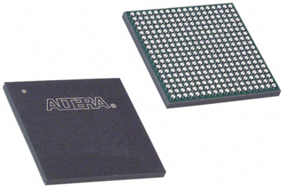
FPGA, Cyclone IV E, INTEL EP4CE6F17I7N, FBGA-256
NCNR (non cancelable / non returnable)
Unit Price (€ / pc.)
22.253 € *
Standard delivery time from the manufacturer is: 6 Weeks
FPGA, EP4CE6F17I7N, Altera
An FPGA is a semiconductor device consisting of a matrix of Configurable Logic Blocks (CLBs) connected through programmable interconnects. The user determines these interconnections by programming SRAM. A CLB can be simple (AND, OR gates, etc) or complex (a block of RAM). The FPGA allows changes to be made to a design even after the device is soldered into a PCB.
Technical specifications
| Filter | Property | Value |
|---|---|---|
| Enclosure | FBGA-256 | |
| Assembly | SMD | |
| Number of LABs/CLBs | 392 | |
| Number of logical elements | 6272 | |
| Memory size | 276.48 kbit | |
| Number of I/Os | 179 | |
| Voltage | 1.15-1.25 V | |
| min. operating temperature | -40 °C | |
| max. operating temperature | 100 °C |
Download
Logistics
| Property | Value |
|---|---|
| MSL | MSL 3 |
| Customs tariff number | 85423990 |
| Original Packaging | Tray with 90 pieces |
| Country of origin | KR |
Compliance
| Property | Value |
|---|---|
| RoHS conform | Yes |
| Date of RoHS guidelines | 3/31/15 |
| SVHC free | No |
| Substance description | Melamine |