IS43TR16640ED-125KBLI | Integrated Silicon Solution INC
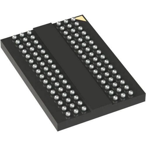
DRAM, 1 Gbit, TFBGA-96, Integrated Silicon Solution INC IS43TR16640ED-125KBLI
NCNR (non cancelable / non returnable)
SDRAM, IS43TR16640ED-125KBLI, Integrated Silicon Solution INC
The Memory controller initiates Leveling mode of all DRAMs by setting bit 7 of MR1 to 1. When entering write leveling mode, the DQ pins are in undefined driving mode. During write leveling mode, only NOP or DESELECT commands are allowed, as well as an MRS command to exit write leveling mode. Since the controller levels one rank at a time, the output of other ranks must be disabled by setting MR1 bit A12 to 1. The Controller may assert ODT after tMOD, at which time the DRAM is ready to accept the ODT signal. The Controller may drive DQS low and DQS# high after a delay of tWLDQSEN, at which time the DRAM has applied on-die termination on these signals. After tDQSL and tWLMRD, the controller provides a single DQS, DQS# edge which is used by the DRAM to sample CK - CK# driven from controller. tWLMRD(max) timing is controller dependent.
Features
- 8 internal banks for concurrent operation
- Programmable CAS Latency
- BL switch on the fly
- Auto Self Refresh(ASR)
- Self Refresh Temperature(SRT)
- Partial Array Self Refresh
- Asynchronous RESET pin
| Filter | Property | Value |
|---|---|---|
| Enclosure | TFBGA-96 | |
| Assembly | SMD | |
| Memory size | 1 Gbit | |
| Voltage | 1.425-1.575 V | |
| Access time | 20 s | |
| Clock frequency | 800 MHz | |
| Technology | SDRAM | |
| min. operating temperature | -40 °C | |
| max. operating temperature | 95 °C |
| Property | Value |
|---|---|
| Customs tariff number | 85423261 |
| MSL | MSL 3 |
| Country of origin | CN |
| Property | Value |
|---|---|
| Date of RoHS guidelines | 3/31/15 |
| RoHS conform | Yes |
| SVHC free | Yes |