Electronics Manufacturing and its Challenges
Electronics manufacturing is a complex matter that presents many challenges. Circuit board assembly in particular presents electronics service providers with great difficulties. How can these challenges be overcome? And how can electronics manufacturing processes be automated in a simple and safe way?
Challenges in circuit board assembly
Not only the advancing digital transformation requires innovative solutions in electronics production. Industry 4.0, the handling of large amounts of data, optimal line integration or increasingly automated line control: topics such as these are also among the major challenges of the present.
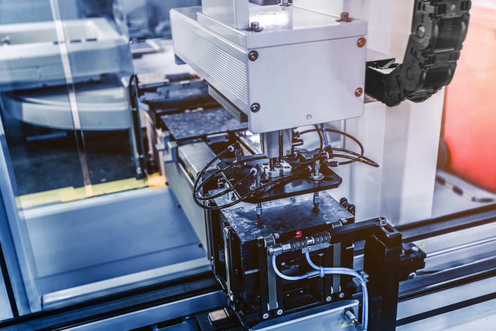
In PCB assembly, individual components are mounted on printed circuit boards. This requires high precision, which trained employees impressively demonstrate time and again. However, humans cannot compete with professional placement machines.
At Bürklin Elektronik, we set ourselves the goal every day of actively supporting you in your electronics manufacturing needs – and have taken a detailed look at the greatest challenges for assemblers below.
Excursus: electronics service providers
Service providers or service companies that develop and produce electronics are called electronics service providers. In English: Electronics Engineering and Manufacturing Services, or E²MS for short.
This also includes electronics manufacturing services (EMS). As manufacturing service providers for electronic components, these companies deal with the complete contract manufacturing of electronic assemblies. Under certain circumstances, EMS can be used to outsource parts of a production process and thus reduce costs.
Fine-pitch assembly
Briefly, the average distance between the connecting legs of electronic components is known as the pitch. If this is less than 0.5 millimeters, it is known as a fine pitch.
Ultra-flat and highly miniaturized components: In fine-pitch assembly, electronics manufacturers work with latest-generation products such as QFN ICs, LGA power components or 03015 chip resistors, among others. This requires extremely precise stencil printing. In contrast, setup, product changeover and cycle times must be kept as short as possible in the interests of high productivity. The challenge lies precisely in this balance.
Crucial for the result: the printing process
An efficient printing process is the be-all and end-all in fine-pitch assembly. If printed circuit boards are found to be defective at the end of production, the printing process is identified as the source of the defect in 70 percent of cases. Overlooking minor details or neglecting process monitoring is out of the question. Speed is always the focus of manufacturers.
Various measures can be taken to improve the increasingly complex printing process. Our recommendations:
- it should be possible to check the correct alignment of the stencil on the printed circuit board as quickly as possible.
- in case of different requirements, it is better to use two stencils with different thicknesses instead of one stencil.
- consider the behavior of the solder paste and adjust the squeegee angle (angle between squeegee and stencil) depending on the paste viscosity.
- maintain print stability with two-lane productivity.
THT placement
The abbreviation THT stands for “Through Hole Technology”, also known as through-hole assembly. It is a special process in PCB assembly: Wired components are inserted with their wire connections into the contact holes of the PCB. The components are then soldered to the conductor track, creating a permanent connection.
The assembly of THT components is a challenge – both in terms of quality and process technology. To a large extent, THT assembly is carried out manually, which increases the time required and increases the number of errors as well as costs. By using the pin-in-paste process, parts of the process can now be automated.
Wondering what the pin-in-paste process is? Pin-in-paste is used to treat and automatically assemble wired components. The following steps are involved:
- filling of the holes on the circuit board with solder paste.
- insertion of the pins of the THT components into the paste-filled holes by the placement machine.
- soldering in the so-called reflow oven. During this process, the tin in the paste – which hangs on the pin as a drop after insertion – is drawn upwards, thus filling the vias.
Automatic optical inspection – the challenges
THT devices can consist of small-format circuits and discrete components – but so can large and massive components on a PCB. This poses challenges for all those working with Automatic Optical Inspection (AOI) inspection technology:
- PCB mass: Various through-hole components on printed circuit boards for high-current and high-power applications result in a weight of several kilograms. Such assemblies are therefore transported in workpiece carriers during production. If these are large and heavy, special roller conveyors are required.
- Design of the workpiece carriers: many workpiece carriers are manufactured in-house, resulting in different dimensions and clamping devices. Accordingly, the position of the printed circuit board also differs.
- Height of the components: Since PCBs are up to 80 mm high, it is important to be able to test both flat and tall components.
- Access to the solder joints of the THT components: The THT solder joints are located on the underside of the PCB. In addition, mounts with cutouts of different shapes, sizes and thicknesses protect the SMD components.
- Mechanical deformation: during soldering, the PCBs are exposed to high temperatures. Downward or upward bulging is a possible consequence.
What is needed is advanced inspection technology. Creating awareness in this regard is already a first step in the right direction.
SMD assembly
Since the 1980s, components have been produced that can be soldered directly onto printed circuit boards by means of a solderable connection surface. They are known as surface mounted devices (SMD), and the associated soldering technology is called surface mount. The soldering process uses reflow and includes wave or surge bath. SMD components are processed as reel stock, belt sections, bar, or tray.
In the meantime, SMD production, i.e. the assembly of SMD components, has developed into an important component of contemporary EMS services. No wonder, after all, this has made it possible so that:
- dense and double-sided assemblies are possible,
- electronic devices can be greatly reduced in size and
- the packing density could be increased.
Flawless soldering required for best results
Only if the soldering of SMD components is flawless can the best product quality be ensured. In times of advancing miniaturization, it is becoming increasingly difficult to inspect printed circuit boards – either with the naked eye or by means of a microscope. Image processing methods (AOI systems), which precisely and quickly check the most important parameters, are sometimes used.
For special cases: Special optics are available for inspecting so-called ball-grid array solder joints, sawed or untreated side surfaces or flat heat-conducting pads: If optical inspection of SMD components is not possible in these or other cases, inspection can only be carried out on a random basis using X-rays.
Challenging work for manual assemblers
SMD technology makes it exceedingly difficult to solder more and more components without machines or know-how. Nevertheless, many component sizes can be processed – with aids such as tweezers, a fine soldering tip, 0.5 mm solder, magnifying glasses and possibly a stereo microscope. Since there is no component preparation, SMD assembly is sometimes even faster compared to manual assembly of wired components.
Important: Classic breadboards and strip grid boards are only of limited use for test setups or prototypes. However, there are suitable laboratory cards and adapters available on the market, which can also be manufactured by the user if required.
Bürklin Elektronik as a reliable partner for EMS services
Whether SMD, THT or mixed assembly: Bürklin Elektronik carries a large number of the most common innovative components for PCB assembly as well as product variants in its portfolio – also in larger quantities, ex stock. We support you at any time and from the very beginning of your project – regardless of whether you have short-term requirements for the production of prototypes and small series or mass production.
We attach great importance to the fulfillment of our delivery promise and the quality of our products. The procurement of high-quality components and printed circuit boards as well as the demand-oriented and thus resource-saving supply for your production are part of our daily business. For this we have access to an extensive supplier network.
This might also interest you
-
Industry 4.0
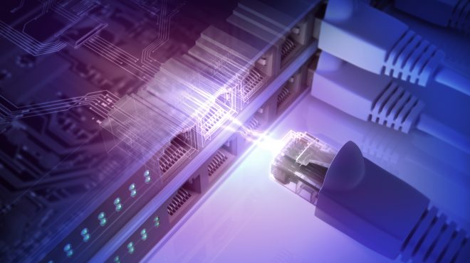
Ethernet: Definition & Guide
You could say that Ethernet forms the backbone of modern network infrastructures. The innovative technology has undergone continuous development since its introduction in the 1970s. This guide provides a comprehensive ov...
-

Industry 4.0
Patch Cables: The Invisible Heroes of Network Connection
Patch cables - unimposing, but indispensable for the smooth functioning of modern networks. The pre-assembled cables with connectors at both ends serve as connecting elements between network devices such as computers, sw...
-
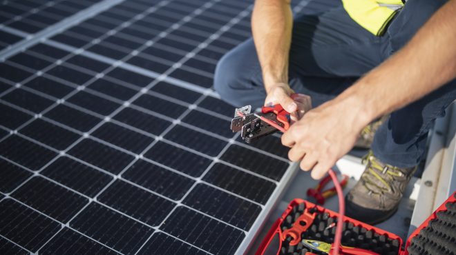
Energy efficiency
Crimping Solar Cables – How to Make the Perfect Connection
Find out how you can connect your solar system perfectly with the right technology and the right tools. We will show you step by step how to make professional crimp connections and thus ensure a safe and efficient power ...